全球領先的壓電技術

通過DLC成膜的等離子控制技術與無機晶體控制技術相結合,我們成功地將被認為極難合成的壓電材料單晶化, 並建立了製造方法。單晶技術能夠應用在各種半導體加工,同時表現出比現有多晶材料更高的性能。
內容:
- The Features of Single-Crystal Thin Film
- Unique Features of KRYSTAL® Wafer's PZT Single-Crystal
- Mechanism of Single-Crystal Deposition by KRYSTAL® Wafer
The Features of Single-Crystal Thin Film
The most distinctive feature of our single crystal technologies is the broad process margin, which is made possible by unique buffer layer technologies.
The buffer layer changes its shape to fill in gaps between the substrate and the crystal lattice of the piezoelectric thin film, creating a single crystal structure with minimal residual stress.
Furthermore, advanced plasma control enables fine-tuning of material characteristics in keeping with the application, with no change in the material composition.
We offer single-crystal piezoelectric thin-film wafers (KRYSTAL® Wafer) for a variety of piezoelectric MEMS applications.

Piezoelectric materials manufactured using basic film structures have the following characteristics:
- They maintain continuous single crystal structures from the silicon (Si) substrate, and reflect single crystal structures without being influenced by the thickness of the piezoelectric thin film
- They have a “ Cube on Cube” structure; that is, a crystal structure somewhat like dice stacked up so they will not roll
- There are few crystal flaws in piezoelectric thin film on strontium ruthenate (SRO), enabling reliable operation even with sub-micron thickness.
These characteristics can be applied not only to PZT (lead zirconate titanate), which is well known as a piezoelectric material, but also to barium titanate (BTO) and numerous other materials as well. Silicon based substrates with a regular (100) orientation are used as a standard, but other orientations have the following characteristics: - When the silicon substrate orientation of <(110) or (111)> is changed, the film orientation can be carried over from the upper layer, providing an optimum combination of materials.
We offer these platforms and proposes ideal combinations to meet the customers’ needs.

Unique Features of KRYSTAL® Wafer's PZT Single-Crystal
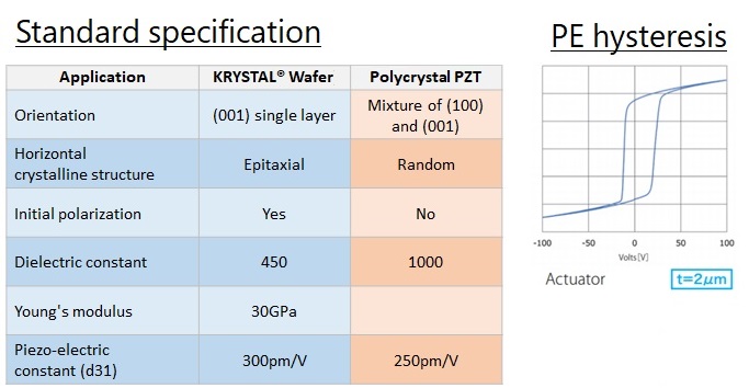
KRYSTAL® Wafer's single-crystal piezoelectric thin films shows superior electrical and mechanical characteristics compared to common poly-crystal piezoelectric thin films.

The most notable features of KRYSTAL® Wafer PZT thin film:
- Single crystal thin film
- Initial polarization from immediately after film forming is maintained
- High heat resistance, with no depolarization even at reflow temperatures (450℃)
- Dielectric constant is less than half compared to polycrystalline materials with similar displacement
-
Superior Electrical and Mechanical Characteristics
The piezoelectric property direction is aligned when single crystalized.
It exhibits superior actuator and sensor performance.

-
Improved reliability
Single crystallization improves the bonding between atoms.
It has approx. 100 times longer life than polycrystal PZT.

Mechanism of Single-Crystal Deposition by KRYSTAL® Wafer
We have successfully reproduced single-crystallization on customer equipment using KRYSTAL® Wafer.
